Cleanrooms are specialized facilities designed to maintain extremely low levels of airborne particles and contaminants. These controlled environments play a critical role in the production of semiconductor devices, ensuring their quality and performance.
Recent breakthroughs in cleanroom technology have revolutionized the semiconductor industry, enabling the development of smaller, faster, and more energy-efficient devices.
In this article, we will explore some key cleanroom advancements that are fueling the next generation of semiconductor devices.
Enhanced Air Filtration Systems
One breakthrough in cleanroom technology is the development of advanced air filtration systems. These systems utilize high-efficiency particulate air (HEPA) filters that can remove particles as small as 0.3 microns in diameter. Additionally, ultra-low penetration air (ULPA) filters are employed, which can eliminate particles as small as 0.12 microns.
These enhanced filtration systems effectively reduce the presence of contaminants in cleanrooms, allowing for the production of highly reliable semiconductor devices. By minimizing particle contamination, these breakthroughs enable the fabrication of increasingly miniaturized components with enhanced performance.
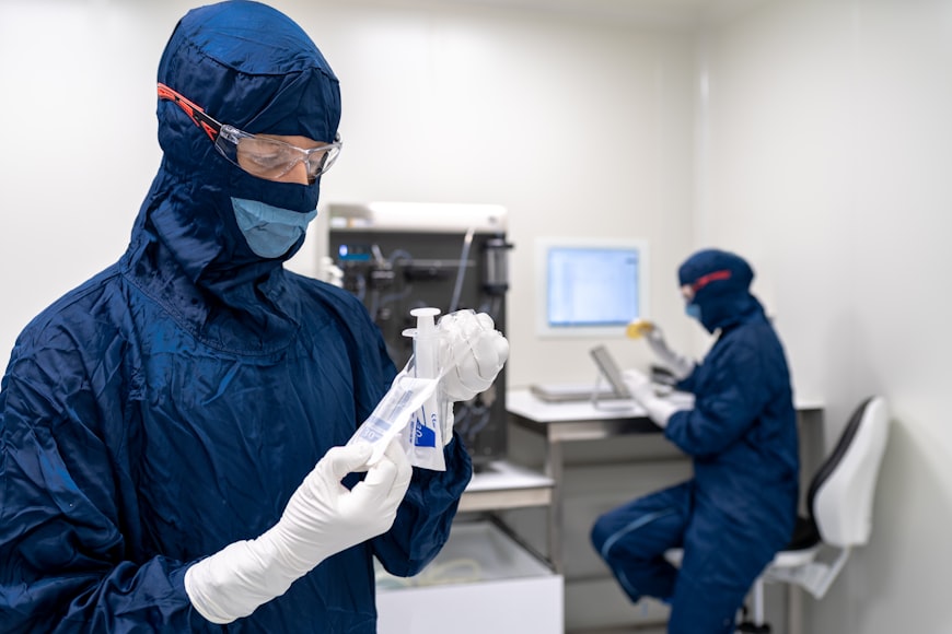
Another area of cleanroom innovation lies in the development of advanced cleanroom garments. These specialized suits are designed to minimize human-generated contamination by effectively trapping particles shed from the body. Recent advancements include the integration of nanotechnology and smart textiles into cleanroom garments.
Furthermore, ergonomic designs and breathable fabrics enhance the comfort and productivity of cleanroom personnel. These advancements in cleanroom garments help maintain the cleanliness of the environment and ensure the integrity of semiconductor manufacturing processes.
Static Dissipative Cleanrooms: Mitigating ESD Risks
According to American Cleanroom Systems, electrostatic discharge (ESD) poses a significant risk in cleanroom environments where sensitive electronic components are manufactured. To address this concern, static dissipative cleanrooms have emerged as a breakthrough in cleanroom technology. These specialized facilities are designed to mitigate ESD risks by incorporating materials and practices that effectively dissipate static charges.
Static dissipative cleanrooms feature conductive flooring, grounded work surfaces, and ionization systems that neutralize electrostatic charges. Conductive flooring materials, such as rubber or epoxy, provide a controlled path for static charge dissipation. Grounded work surfaces and ionization systems further aid in the removal of electrostatic charges from personnel and equipment.
Cleanroom Automation and Robotics
Automation and robotics have become crucial elements in modern cleanroom environments. Cleanroom automation systems reduce human intervention and limit the potential for contamination. Robots equipped with precise motion control capabilities can perform delicate tasks such as wafer handling, pick-and-place operations, and equipment maintenance.
Moreover, cleanroom robots are designed with materials that minimize particle shedding and are compatible with cleanroom protocols. The integration of automation and robotics improves process efficiency, accelerates production rates, and enhances the overall cleanliness and safety of the cleanroom environment.
Cleanroom monitoring and control systems have evolved significantly, enabling real-time tracking and regulation of environmental conditions. These systems employ sensors that measure crucial parameters such as temperature, humidity, air pressure, and particle concentration.
According to a blog article by News Medical, excellent cleanroom air quality is critical to ensuring the quality of the product being produced or the successful completion of the procedure being done in the cleanroom. Airborne sampling is required to assess if the cleanroom meets the universal standard.
Advanced algorithms and data analysis techniques provide insights into the cleanroom environment’s stability and allow for immediate adjustments to maintain optimal conditions. Real-time monitoring ensures that semiconductor fabrication processes are carried out under controlled parameters, leading to consistent quality and yield improvement.
Nano-scale Cleaning Techniques
The miniaturization of semiconductor devices necessitates the development of nano-scale cleaning techniques to remove contaminants at the atomic and molecular levels. These techniques effectively remove sub-nanometer-sized particles and thin films from critical surfaces.
Additionally, the use of environmentally friendly cleaning agents reduces the impact on the ecosystem. Nano-scale cleaning techniques contribute to the production of defect-free semiconductor devices, allowing for the fabrication of cutting-edge processors, memory chips, and sensors.
According to a study published in the Nature Journal, atomic layer deposition (ALD) has emerged as a breakthrough technique in the semiconductor industry, enabling the deposition of thin films with atomic-level accuracy. This technique is crucial for the development of advanced semiconductor devices. ALD’s atomic-level precision and excellent film uniformity make it an indispensable tool for semiconductor manufacturers
Integration With Renewable Energy
As the semiconductor industry continues to grow, the demand for cleanroom energy consumption increases. To address this challenge, cleanroom facilities are integrating renewable energy sources to reduce their environmental footprint. Solar panels, wind turbines, and energy-efficient lighting systems are being installed to generate clean electricity.
In addition, advanced energy management systems play a crucial role in optimizing energy usage to maximize the efficiency of cleanrooms. Airflow optimization is fundamental in this regard. An article by Cleanroom Technology highlights the significance of heating, ventilation, and air conditioning (HVAC) within the cleanroom system, as it accounts for up to 70% of a site’s energy consumption.
This presents a tremendous opportunity for energy and carbon reduction, particularly through reducing the air change rate. Even minor decreases in airflow can yield significant outcomes. For example, a mere 10% reduction in airflow can result in a substantial 28% decrease in fan power consumption.
These initiatives not only reduce carbon emissions but also enhance the sustainability of semiconductor manufacturing. By adopting renewable energy solutions, cleanroom facilities contribute to the development of eco-friendly semiconductor devices.
Recent advances in cleanroom technology are catapulting the semiconductor industry into a new era of invention. Among the key advancements that are revolutionizing semiconductor device fabrication are advanced air purification systems, specialized cleanroom garments, static dissipative cleanrooms, robotics and automation, advanced monitoring methods, nano-scale cleaning techniques, and integration with energy from sustainable sources.
These advancements have led to the development of extremely dependable, downsized components with improved performance. They have also increased cleanroom process efficiency, sanitation, and safety. The semiconductor industry is ready to produce cutting-edge processors, memory modules, and sensors that will impact the future of technology by leveraging these innovations.

